Thunderbolt 5 is Here - Up To 80 Gbps Bandwidth With Existing USB Type-C Ports

Gregory Bryant, Executive Vice President and General Manager of Intel’s Client Computing Group, is visiting the Israeli Intel Research and Development facilities in an effort to see what new products and technologies are in development for the future of Intel such as the next-gen Thunderbolt Type-C interface.

Intel Accidently Unveils Thunderbolt 5 (PAM-3 Modulation) Technology With Up To 80 Gbps Transfer Speeds
Like most executives, he is documenting part of his trip through social media, namely Twitter. Posting to social media is great for public relations, but is also full of room for error. While visiting one of the Israeli facilities, several photos were taken, and he posted some for Intel fans and users on Twitter. One photo which shows Intel's Next-gen Thunderbolt 5 technology with PAM3 made it to Twitter, along with a few others, but was promptly removed and replaced with only three photos from the visit.
Why was the post removed? The photo in question displayed information on a poster at the facility that showcased new technology that was not meant to be released to the public—at least not yet.
The subject of the poster states "80G PHY Technology", which is speculated to be the physical layers on an 80 Gbps connection. If this is true, that is currently double the current physical layers, which is 40 Gbps, utilizing Thunderbolt 4.
Underneath the header, the first line reads "[The U]SB 80G is targeted to support the existing USB-C ecosystem". With this information, Intel plans to continue with the USB-C connections, which is almost completely the standard for most technology connections, for the new technology. The biggest change is that the bandwidth is now doubled.
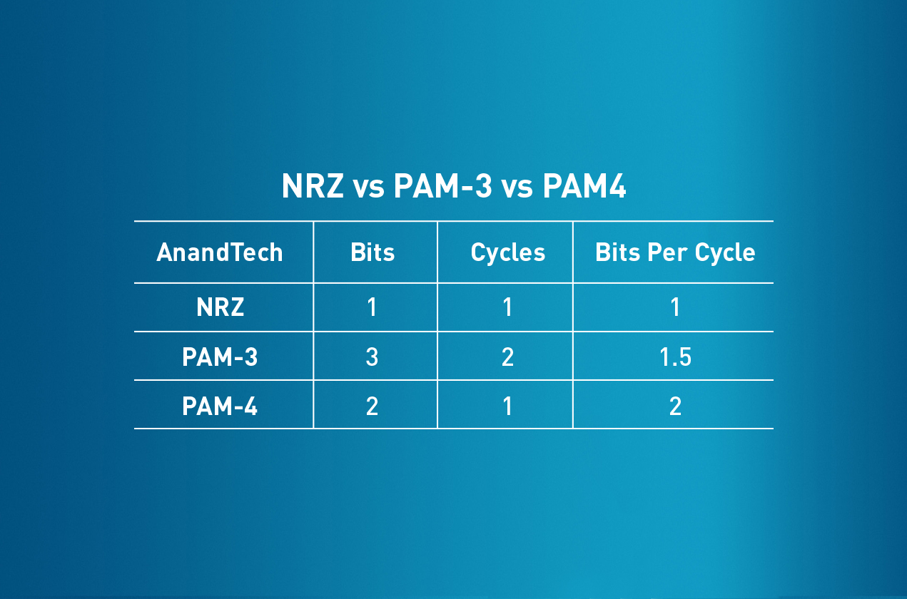
The following line reads "[T]he PHY will be based on novel PAM-3 modulation technology". When talking about PAM-3, or Pulse Amplitude Modulation, we are discussing how 0s and 1s are transmitted, or in this case, a single bit. Right now, PAM-4 and NRZ are the standard, where the number 4 pertains to the number of variances of zeros and ones (00, 01, 10, or 11) being transmitted in NRZ, or a single bit.
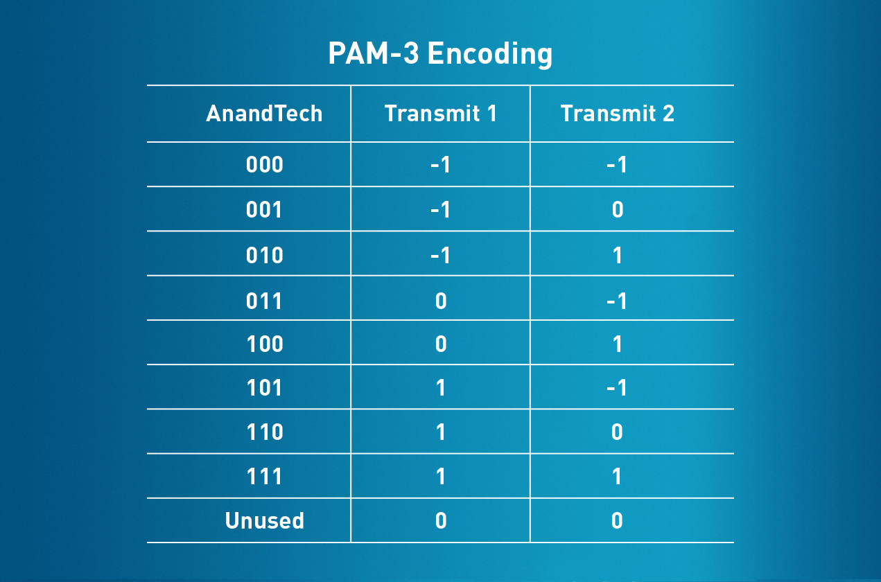
In PAM-3, zeroes and ones are thought of in negative or positive values—i.e. -1, 0, and +1. The system then combines two PAM-3 modules and transmits the information into 3-bit data signals, where the value 000 is an -1 followed by -1.
So, where PAM-4 is twice the bandwidth of NRZ, PAM-3 is in between the two but allows for a much higher bandwidth that PAM-4 needs to utilize exceptions and extra limitations. In essence, this technology will process the variables, not only faster but more efficiently.
The last visible line states "[...]N6 test-chip focusing on the new PHY technology is working in [...] showing promising results". The only information that can be gathered by the statement is that the N6 test-chip is a TSMC node. Outside of that, it is unsure what the complete statement shows.
Advancing to a Thunderbolt 5 bandwidth seems the most logical step for Intel to move towards, but with only having the information provided, we will have to wait until we can access more information to provide an expert opinion on Intel's move towards PAM-3 technology.


